From smartphones and computers to electric cars and airplanes, solder joints, semiconductor packages and electrical components are vital to so many of our most important devices. Waygate Technologies brings high resolution 2D X-ray and 3D Computed Tomography (CT) inspection solutions right to the electronics production line and the research and development lab to ensure the safety and integrity of components.

Meet strict requirements and reduce human factor in manufacturing and maintenance

A key trend arising from the pandemic and growth in raw-material-intensive markets (batteries) is security of supply.

Printed circuit boards, connectors, consumer electronics, and more require a high level of precision and resolution in the manufacturing and testing.

A surge from every sector and industry, including personal and wearable devices, has increased the demand for electronics and their corresponding raw materials.

With the supply and demand increase of electronics, the reuse and recycling of these electronics is still questionable ... More needs to be done in this circular economy.
We deliver smart, productive, and lean inspection solutions for the electronics industry
Technologies made for your industry challenges

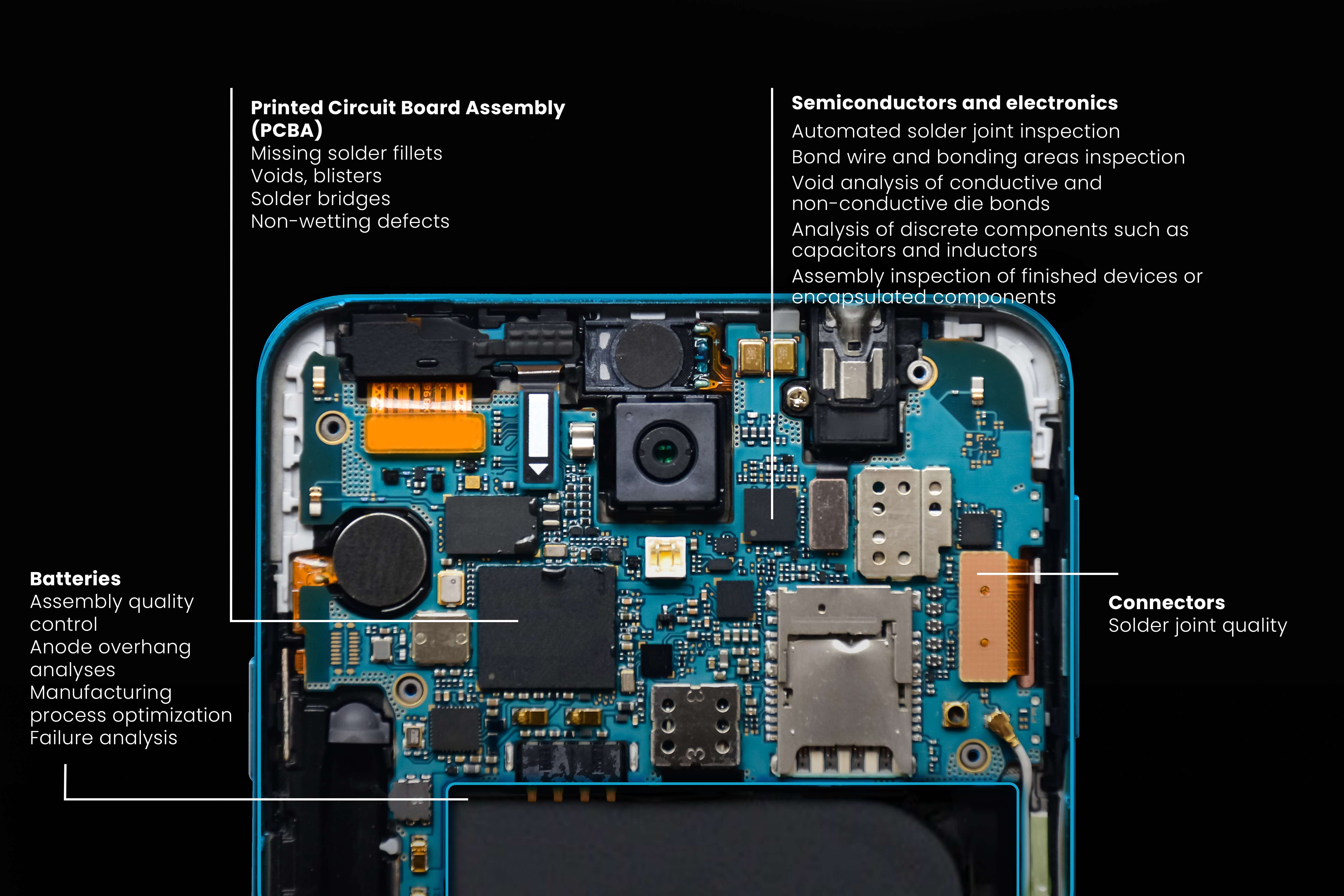
Li-ion batteries are among the most powerful energy storage devices commonly used in portable electronic devices, stationary power sources and electric vehicles. Our broad portfolio of premium radiography systems supports not only R&D as well as the post-mortem analysis of defective li-ion batteries to analyze the means of failure, but also fast CT inspection providing safe and secure production control with a reliable inspection of all vital parts.

Because electronic components are becoming increasingly miniature and even more complex, high-resolution X-ray inspection has become a widely used tool for non-destructive failure analysis and process control in a variety of industrial and scientific fields. Our powerful nano- and microfocus X-ray technologies provide the means necessary to detect even the most minute defects in solder joints, bond wires and bonding areas, conductive and non-conductive die bonds, capacitors and inductors, finished assembly inspections, and more.

High-resolution X-ray technology is widely used in failure analysis and production quality testing of electronic devices to achieve more accurate inspections. Where standard 2D AXI does not allow reliable results due to overlaying features, our nano- and microfocus X-ray technologies provide clear slice views of packages or PCBSs. Any material flaw and quality characteristic affecting the shape of solder joints can be detected, like missing solder fillets, voids and blisters, solder bridges, or non-wetting defects.

For 3D evaluation of the smallest details with the highest resolution, our advanced CT scanners and nano- and microfocus X-ray technologies bring extremely precise inspections usually reserved for research and quality labs to fast moving production lines. Combined with AI-based automated defect recognition algorithms (for applications like anode overhang analysis in batteries, our systems can be fully integrated into your electronics production line to ensure the highest quality and efficiency.


